Metallisation - Interconnects
Students: M. Thomas, R. Bouyssou
Objectives
In the " Metallisation - Interconnects" research program, studies are made on materials
for contacts and interconnects in silicon based integrated circuit technology. The first topic is related
to copper deposition for interconnects and related materials for diffusion barrier. Additionally, the demand
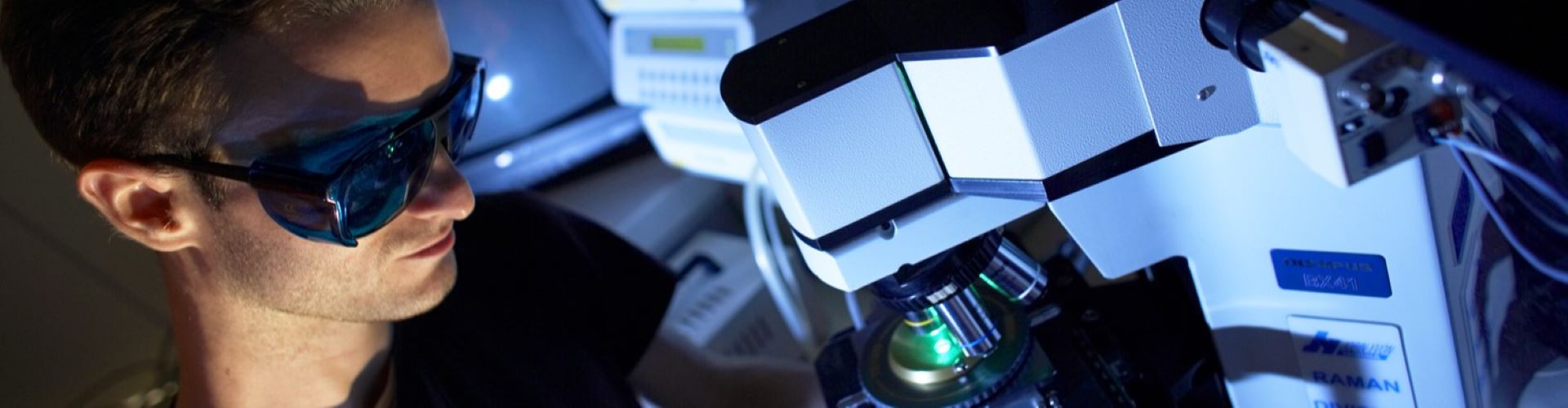
from the contributors to advanced integration is increasingly higher for structural examination at the atomic
scale of patterned thin films. Thus, numerous structural studies are conducted by transmission electron
microscopy from materials for micro/nano-electronics applications. The studies are designed from the outset, to feed into programmes at the CEA's LETI laboratory
and/or at STMicroelectronics, under contractual partnerships which are strongly supported by the associated institutions.
Main Results
- Characterization and development of 3D architecture for Metal- Insulator-Metal capacitors integrating copper electrode and high-! dielectrics. Ph-D : M. Thomas The current scaling down of IC dimensions also applies to passive components integrated among Cu interconnects, such as Metal-Insulator-Metal (MIM- ca pacitors. A new solution is required to reach high capacitance densities, keep good performance levels and ensure the compatibility of MIM capacitors with the BEOL (Back End Of Line). A new architecture was developed for MIM capacitors targeting analog and RF applications. The Ta2O5 dielectrics deposited by PEALD (Plasma Enhanced Atomic layer Deposition) was associated with TiN electrodes and TaN / Ta diffusion barriers in a damascene 3D architecture with highly developed area, resulting in capacitance densities higher than 15 fF/!m2 This MIM capacitor was completely characterized by extensive physico-chemical analysis and electrical measurements. Stack simplification and performance improvement were proposed by using electrode modification and dielectric multistacking. High-frequency measurements and electromagnetic simulations resulted in design and process recommendations to meet high-performance request of MIM capacitors
- Extendability of PVD methods to advanced CMOS copper interconnect technologies (Collaboration STMicroélectronics- Crolles) - Thèse R. BouyssouIn advanced IC technologies, dielectric materials are used to ensure electrical insulation between copper interconnects. A barrier layer is deposited to prevent copperof diffusing into dielectrics. On top of this layer aso-called "seed layer" is deposited to permit further copper electro-filling of interconnects. Physical VapourDeposition (PVD) methods are used to obtain these layers. However in regards of the deposition performance requested by the high geometry aspect-ratio involved in advanced technology, PVD methods have to be demonstrated as adapted to these highly demanding challenges. In the thesis work it was demonstrated that experimental adaptations of the deposition methods may permit to use PVD in 32 and 22 nm technologies.
Staff
B. Chenevier
J.M. Dedulle