Papier de Hongjun Liu
Le papier "Visualization of nanocrystalline CuO in the grain boundaries of Cu2O thin films and effect on band bending and film resistivity" a été publié dans APL Materials.
Ici vous trouverez le papier de Honjun
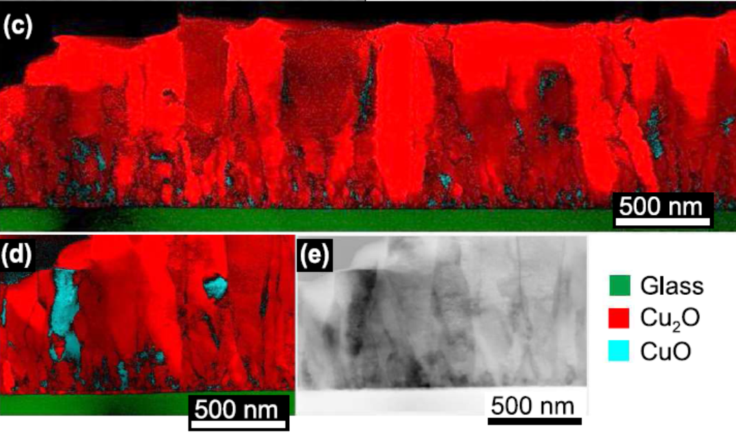
"Direct evidence for the presence of a CuO structure in the grain boundaries of Cu2O thin films by chemical vapor deposition is provided by high resolution automated phase and orientation mapping (ASTAR), which was not detectable by classical transmission electron microscopy techniques. Conductive atomic force microscopy (CAFM) revealed that the CuO causes a local loss of current rectification at the Schottky barrier between the CAFM tip and Cu2O. The suppression of CuO formation at the Cu2O grain boundaries is identified as the key strategy for future device optimization."