New paper by Evgenie Skopin 2018
The paper "The initial stages of ZnO atomic layer deposition on atomically flat In0.53Ga0.47As substrates" has been published in Nanoscale
Here you will find the paper by Evgenie Skopin
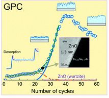
"InGaAs is one of the III–V active semiconductors used in modern high-electron-mobility transistors or high-speed electronics. ZnO is a good candidate material to be inserted as a tunneling insulator layer at the metal–semiconductor junction. A key consideration in many modern devices is the atomic structure of the hetero-interface, which often ultimately governs the electronic or chemical process of interest. Here, a complementary suite of in situ synchrotron X-ray techniques (fluorescence, reflectivity and absorption) as well as modeling is used to investigate both structural and chemical evolution during the initial growth of ZnO by atomic layer deposition (ALD) on In0.53Ga0.47As substrates. Prior to steady-state growth behavior, we discover a transient regime characterized by two stages. First, substrate-inhibited ZnO growth takes place on InGaAs terraces. This leads eventually to the formation of a 1 nm-thick, two-dimensional (2D) amorphous layer. Second, the growth behavior and its modeling suggest the occurrence of dense island formation, with an aspect ratio and surface roughness that depends sensitively on the growth condition. Finally, ZnO ALD on In0.53Ga0.47As is characterized by 2D steady-state growth with a linear growth rate of 0.21 nm cy−1, as expected for layer-by-layer ZnO ALD."