OBJECTIVES
To exploit the functionalities of nanowires through collective use within nanonets.
To exploit the functionalities of nanowires through collective use within nanonets.
Highlight
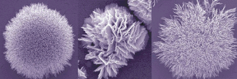
Based on a simple and versatile fabrication method, the collective use and integration of high aspect ratio nanostructures, such as carbon nanotubes and Si or ZnO nanowires (NWs), leads to nano-size networks (nanonets).
The nanonets address multiple application fields, including transparent conducting material, light detection, active material for bio-sensing devices, or materials with interesting wettability properties.
In particular, by combining sol-gel protocols and hydrothermal synthesis, well controlled ZnO NWs are grown for further integration in nanonets.
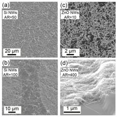
Si (left a-b) and ZnO nanonets (right c-d). The mechanical flexibility of these nanonets is illustrated in (d) for a ZnO nanonet deposited across a 500 nm SiO2 step.
The nanonets address multiple application fields, including transparent conducting material, light detection, active material for bio-sensing devices, or materials with interesting wettability properties.
In particular, by combining sol-gel protocols and hydrothermal synthesis, well controlled ZnO NWs are grown for further integration in nanonets.
Si (left a-b) and ZnO nanonets (right c-d). The mechanical flexibility of these nanonets is illustrated in (d) for a ZnO nanonet deposited across a 500 nm SiO2 step.
Contact
FM2N Research topics
- Nanowires, Thin Films & Heterostructures as ...
- Wet Chemistry & Surface Functionalization
- Transparent Conducting Materials
- Physical Chemistry at Interfaces, advanced structural characterization
Main publications
P. Serre, M. Mongillo, P. Periwal, T. Baron and C. Ternon,
Percolating silicon nanowire networks with highly reproducible electrical properties, Nanotechnology (26) 015201 (2015), doi:10.1088/0957-4484/26/1/015201.
C. Ternon, P. Serre, G. Rey, C. Holtzinger, P. Periwal, M. Martin, T. Baron, V. Stambouli and M. Langlet,
High aspect ratio semiconducting nanostructure random networks: highly versatile materials for multiple applications, Phys. Status Solidi RRL, 7(10) (2013) 919.
P. Serre, C. Ternon, V. Stambouli, P. Periwal and T. Baron,
Fabrication of silicon nanowire networks for biological sensing, Sensors and Actuators B 182 (2013) 390.