OBJECTIVES
NON PERMANENT STAFF
COLLABORATIONS
Development & use of ZnO nanowires for electronic, optoelectronic, and photovoltaic devices:
- Understanding the formation and doping mechanisms of ZnO nanostructures (nanoparticles, nanowires) grown by chemical deposition techniques (wet chemistry, CVD, ALD).
- Integrating ZnO nanowires in new heterostructures combining different types of compound semiconductors.
- Fabricating ZnO nanowire-based advanced devices with a special emphasis on the third generation solar cells.
NON PERMANENT STAFF
- Sophie Guillemin (PhD student)
- Jérôme Michallon (PhD student)
- Romain Parize (PhD student)
- Claire Verrier (PhD student)
- Amandine Bocheux (Post-Doc)
- Stéphane Brochen (Post-Doc)
COLLABORATIONS
- IMEP-LAHC, Grenoble (France)
- Institut Néel & CEA-INAC with Equipe Mixte « Nanophysique et Semiconducteurs », Grenoble (France)
- CEA-LETI, Grenoble (France)
- INL, Institut des Nanotechnologies de Lyon (France),
- LEPMI-MOPS, Le Bourget-du-Lac (France)
- SIMaP, Saint-Martin-d'Hères (France)
- LTM, Grenoble (France)
- Institut Jaume Almera, CSIC, Barcelona, Catalonia (Spain)
Contact
Team (Permanent Staff)
Projects
- CELESTE – Bonus Qualité Recherche grant from Grenoble INP (2011-2014)
- CLAPE – Institut Carnot Energies du Futur (2013-2015)
- ARC 6 – Région Rhône-Alpes - (2011-2014)
- Labex CEMAM IRP2& IRP5 (2014-2017)
- ANR MetalliGaN (2013-2016)
FM2N Research topics
- Nanowires, Thin Films & Heterostructures as ...
- Wet chemistry & surface functionalization
- Transparent Conducting Materials
- Physical chemistry at interfaces, advanced structural characterization
Highlight
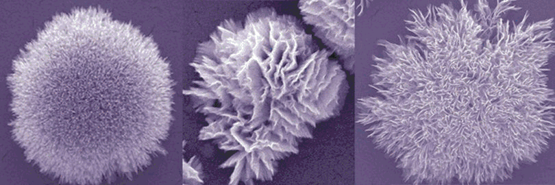
Controlling the polarity in addition to the structural uniformity of ZnO nanowires is critical for real-world-device integration. We have recently demonstrated, by combining selective area growth with chemical bath deposition, the fabrication of epitaxial ZnO nanowire arrays with great structural uniformity and optical quality as well as with controllable polarity. These open new opportunities for fabricating complex heterostructures for electronic, optoelectronic and photovoltaic devices.
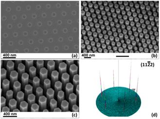
(b), (c) Tilted-view FESEM images of ZnO nanowires grown by chemical bath deposition on patterned O-polar c-plane ZnO single crystals.
(d) Corresponding x-ray pole figures recorded on the (112 ?2) asymmetric diffraction peak of ZnO nanowires.
Main publications
V. Consonni, G. Rey, J. Bonaimé, N. Karst, B. Doisneau, H. Roussel, S. Renet, D. Bellet
Synthesis and physical properties of ZnO/CdTe core shell nanowires grown by low-cost deposition methods, Appl. Phys. Lett. 98, 111906 (2011).
E. Puyoo, G. Rey, E. Appert, V. Consonni, D. Bellet
Efficient Dye-Sensitized Solar Cells Made from ZnO Nanostructure Composites, J. Phys. Chem. C 116, 18117 (2012).
S. Guillemin, V. Consonni, E. Appert, E. Puyoo, L. Rapenne, H. Roussel
Critical Nucleation Effects on the Structural Relationship Between ZnO Seed Layer and Nanowires, J. Phys. Chem. C, 116, 25106 (2012).
S. Guillemin, L. Rapenne, H. Roussel, E. Sarigiannidou, G. Brémond, V. Consonni
Formation Mechanisms of ZnO Nanowires: The Crucial Role of Crystal Orientation and Polarity, J. Phys. Chem. C 117, 20738 (2013).
V. Consonni, E. Sarigiannidou, E. Appert, A. Bocheux, S. Guillemin, F. Donatini, I.C. Robin, J. Kioseoglou, F. Robaut
Selective area growth of well-ordered ZnO nanowire arrays with controllable polarity, ACS Nano 8, 4761 (2014).
Books
 Wide Band Gap Semiconductor Nanowires, Wiley-ISTE, July 2014
 Editors : Vincent Consonni, Guy Feuillet / 2 volumes :